[ad_1]
This sponsored article is delivered to you by COMSOL.
The fashionable internet-connected world is usually described as wired, however most core community information visitors is definitely carried by optical fiber — not electrical wires. Regardless of this, present infrastructure nonetheless depends on many electrical sign processing parts embedded inside fiber optic networks. Changing these parts with photonic gadgets might increase community pace, capability, and reliability. To assist understand the potential of this rising expertise, a multinational crew on the Swiss Federal Institute of Know-how Lausanne (EPFL) has developed a prototype of a silicon photonic part shifter, a tool that might turn out to be a necessary constructing block for the following technology of optical fiber information networks.
Lighting a Path Towards All-Optical Networks
Utilizing photonic gadgets to course of photonic alerts appears logical, so why is that this strategy not already the norm? “An excellent query, however truly a tough one to reply!” says Hamed Sattari, an engineer presently on the Swiss Middle for Electronics and Microtechnology (CSEM) specializing in photonic built-in circuits (PIC) with a deal with microelectromechanical system (MEMS) expertise. Sattari was a key member of the EPFL photonics crew that developed the silicon photonic part shifter. In pursuing a MEMS-based strategy to optical sign processing, Sattari and his colleagues are benefiting from new and rising fabrication expertise. “Even ten years in the past, we weren’t capable of reliably produce built-in movable constructions to be used in these gadgets,” Sattari says. “Now, silicon photonics and MEMS have gotten extra achievable with the present manufacturing capabilities of the microelectronics trade. Our objective is to show how these capabilities can be utilized to rework optical fiber community infrastructure.”
Optical fiber networks, which make up the spine of the web, depend on many electrical sign processing gadgets. Nanoscale silicon photonic community parts, similar to part shifters, might increase optical community pace, capability, and reliability.
The part shifter design challenge is a part of EPFL’s broader efforts to develop programmable photonic parts for fiber optic information networks and house functions. These gadgets embrace switches; chip-to-fiber grating couplers; variable optical attenuators (VOAs); and part shifters, which modulate optical alerts. “Present optical part shifters for this utility are usually cumbersome, or they undergo from sign loss,” Sattari says. “Our precedence is to create a smaller part shifter with decrease loss, and to make it scalable to be used in lots of community functions. MEMS actuation of movable waveguides might modulate an optical sign with low energy consumption in a small footprint,” he explains.
How a Movable Waveguide Helps Modulate Optical Indicators
The MEMS part shifter is a classy mechanism with a deceptively simple-sounding goal: It adjusts the pace of sunshine. To shift the part of sunshine is to sluggish it down. When gentle is carrying an information sign, a change in its pace causes a change within the sign. Fast and exact shifts in part will thereby modulate the sign, supporting information transmission with minimal loss all through the community. To vary the part of sunshine touring by way of an optical fiber conductor, or bus waveguide, the MEMS mechanism strikes a bit of translucent silicon known as a coupler into shut proximity with the bus.
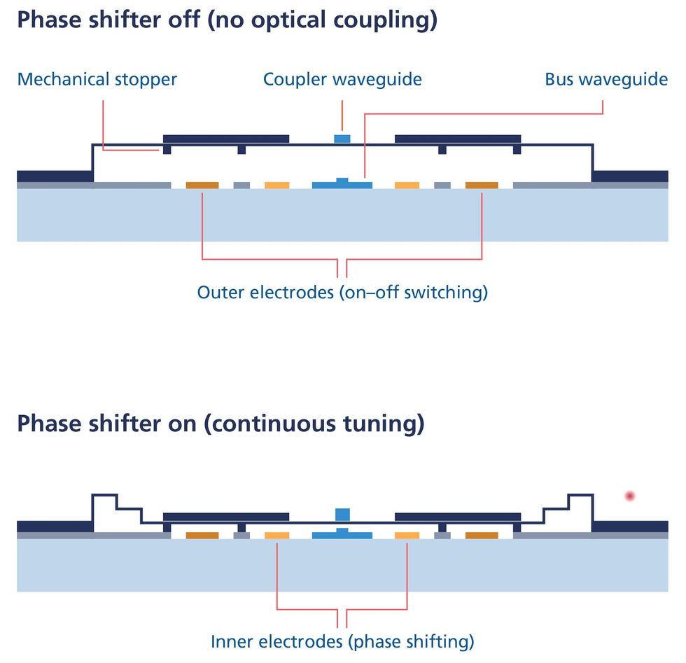
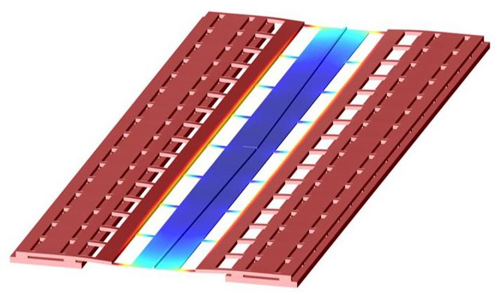
The design of the MEMS mechanism within the part shifter supplies two phases of movement (Determine 1). The primary stage supplies a easy on–off motion of the coupler waveguide, thereby partaking or disengaging the coupler to the bus. When the coupler is engaged, a finer vary of movement is then offered by the second stage. This permits tuning of the hole between the coupler and bus, which supplies exact modulation of part change within the optical sign. “Shifting the coupler towards the bus is what adjustments the part of the sign,” explains Sattari. “The coupler is comprised of silicon with a excessive refractive index. When the 2 parts are coupled, a light-weight wave shifting by way of the bus may also go by way of the coupler, and the wave will decelerate.” If the optical coupling of the coupler and bus will not be rigorously managed, the sunshine’s waveform will be distorted, probably dropping the sign — and the information.
Designing at Nanoscale with Optical and Electromechanical Simulation
The problem for Sattari and his crew was to design a nanoscale mechanism to regulate the coupling course of as exactly and reliably as attainable. As their part shifter would use electrical present to bodily transfer an optical aspect, Sattari and the EPFL crew took a two-track strategy to the gadget’s design. Their objective was to find out how a lot voltage needed to be utilized to the MEMS mechanism to induce a desired shift within the photonic sign. Simulation was a necessary software for figuring out the a number of values that will set up the voltage versus part relationship. “Voltage vs. part is a fancy multiphysics query. The COMSOL Multiphysics software program gave us many choices for breaking this massive downside into smaller duties,” Sattari says. “We performed our simulation in two parallel arcs, utilizing the RF Module for optical modeling and the Structural Mechanics Module for electromechanical simulation.”
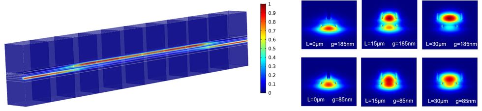
The optical modeling (Determine 2) included a mode evaluation, which decided the efficient refractive index of the coupled waveguide components, adopted by a research of the sign propagation. “Our objective is for gentle to enter and exit our gadget with solely the specified change in its part,” Sattari says. “To assist obtain this, we will decide the eigenmode of our system in COMSOL.”

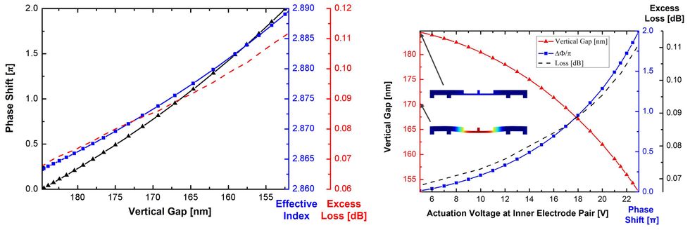
Together with figuring out the bodily types of the waveguide and actuation mechanism, simulation additionally enabled Sattari to review stress results, similar to undesirable deformation or displacement attributable to repeated operation. “Each choice in regards to the design relies on what the simulation confirmed us,” he says.
Including to the Basis of Future Photonic Networks
The objective of this challenge was to show how MEMS part shifters could possibly be produced with present fabrication capabilities. The consequence is a sturdy and dependable design that’s achievable with present floor micromachined manufacturing processes, and occupies a complete footprint of simply 60 μm × 44 μm. Now that they’ve a longtime proof of idea, Sattari and his colleagues look ahead to seeing their designs built-in into the world’s optical information networks. “We’re creating constructing blocks for the long run, and it will likely be rewarding to see their potential turn out to be a actuality,” says Sattari.
References
- H. Sattari et al., “Silicon Photonic MEMS Part-Shifter,” Optics Categorical, vol. 27, no. 13, pp. 18959–18969, 2019.
- T.J. Seok et al., “Giant-scale broadband digital silicon photonic switches with vertical adiabatic couplers,” Optica, vol. 3, no. 1, pp. 64–70, 2016.
[ad_2]
No Comment! Be the first one.