[ad_1]
Nvidia says it has discovered a method to pace up a computation-limited step within the chipmaking course of in order that it occurs 40 occasions as quick as in the present day’s commonplace. Known as inverse lithography, it’s a key instrument that enables chipmakers to print nanometer-scale options utilizing gentle with an extended wavelength than the dimensions of these options. Inverse lithography’s use has been restricted by the huge dimension of the wanted computation. Nvidia’s reply, cuLitho, is a set of algorithms designed to be used with GPUs, turns what has been two weeks of labor into an in a single day job.
The know-how “will enable fabs to extend throughput, scale back their carbon footprint, and set the foundations for 2-nanometer [manufacturing processes] and past,” stated Nvidia CEO Jensen Huang on the Nvidia GTC developer convention on Tuesday.
Main logic-chip foundry Taiwan Semiconductor Manufacturing Co. (TSMC) can be qualifying cuLitho’s use in manufacturing beginning in June, stated Huang. Design automation software program agency Synopsys plans to combine software program, too, and lithography tools maker ASML plans to assist cuLitho in its merchandise as effectively.
Photolithography is principally step one within the chipmaking course of. It includes bouncing gentle off of a sample known as a photomask to challenge the types of transistor buildings and interconnects onto the wafer. (Extra mature know-how makes use of transmissive photomasks as a substitute of reflective ones, however the thought is similar.) It takes 98 photomasks to make an H100 GPU, Jensen stated. The options projected from the photomask are smaller than the wavelength of sunshine used—193 nanometers for the comparatively giant options and 13.5 nm for the finer bits. So, with out the help of tips and design guidelines—collectively known as optical proximity correction—you’d get solely a blurry mess projected onto the wafer. However with optical proximity correction, the designs on the photomask solely vaguely resemble the sample of sunshine on the chip.
With the necessity for finer and finer options, the corrected shapes on the photomask have turn into increasingly more elaborate and troublesome to give you. It might be significantly better to begin with the sample you need on the wafer after which calculate what sample on the photomask would produce them. Such a scheme is known as inverse lithography. Easy because it sounds, it’s fairly troublesome to compute, usually taking weeks to compile.
In reality, it’s such a slog that it’s usually reserved to be used on just a few vital layers of modern chips or simply significantly thorny bits of them, in line with knowledge from the E-Beam Initiative, which periodically surveys the business.
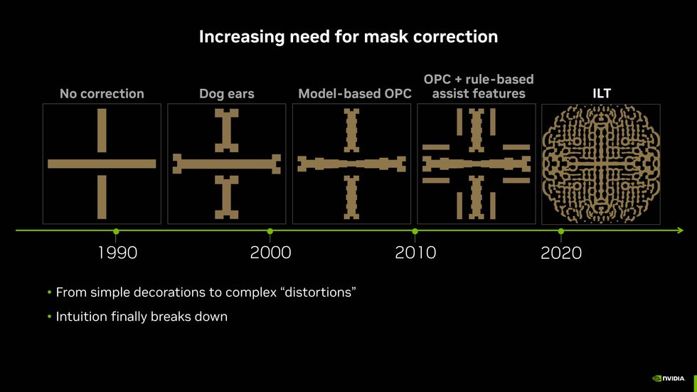 As chipmaking required finer and finer options, engineers needed to produce increasingly more advanced designs to challenge these options onto the silicon. Inverse lithography (ILT) is the newest growth.Nvidia
The lengthy computation time for lithography slows the event and enchancment of chip know-how Even a change to the thickness of a fabric can result in the necessity for a brand new set of photomasks, notes Vivek Okay. Singh, vice chairman within the superior know-how group engaged on silicon manufacturing at Nvidia. Computing masks “has been an extended pole in chip growth,” he says. “If inverse lithography know-how have been sped up 40 occasions, would extra firms apply it to extra layers? Absolutely.”
A part of the computation is a picture drawback that’s a pure match for GPUs, says Singh. However at most, that may solely reduce the computation time in half. The remaining will not be really easy to make parallel. However over the previous 4 years, with growth companions together with TSMC, Nvidia engineers have give you a group of algorithms for making the remaining work parallel and have packaged it as a software program library to be used with GPUs.
In accordance with Nvidia, utilizing the cuLitho lets 500 Nvidia DGX H100 computer systems do the work of 40,000 CPU methods. It may well produce three to 5 occasions as many photomasks per day, drawing solely 5 megawatts as a substitute of 35 MW.
What’s extra, the know-how might ship higher outcomes, in line with Singh. CuLitho produces in any other case hard-to-calculate curvy polygons on the masks, which leads to a higher depth of focus for the sample forged onto the wafer. That depth of focus ought to result in much less variation throughout the wafer and subsequently a higher yield of working chips per wafer, he says. In future, it additionally might imply fewer photomasks are wanted; with inverse lithography, what should now be accomplished with a double sample would possibly work with just one.
Nvidia will not be the primary to look to GPUs to speed up inverse lithography know-how. Silicon Valley-based D2S introduced a GPU-based pc customized constructed for the issue in 2019. IEEE Spectrum reached out to D2S for remark, however the firm didn’t reply earlier than press time.
From Your Website Articles
Associated Articles Across the Internet
[ad_2]
No Comment! Be the first one.